As an example, consider the design of a third-order Chebyshev lowpass
filter with 0.18dB passband ripple, a 1MHz bandwidth and 80dB dynamic range.
The following FA input file is a start.
chebyshev(3, 0.18);
transform: scale;
ctot = 3e-12;
noisefactor = 2;
umax = 1;
output: dr;
It is always a good idea to scale the filter for optimal dynamic range, so the input file contains a scale command. The total capacitance value is an initial guess. The noise factor is 2, or 3dB. Practice shows that this is a reasonable estimate. The maximum RMS single-ended integrator output signal level is 1V. FA generates the following output.
Output noise level: 2.389684e-04 V.
Scaling is L-infinity.
Maximum output level: 1.000000e-00 V.
Dynamic range: 4.184654e+03 (72.43 dB).
The dynamic range is 72.43dB, which is 7.57dB too little. To increase the dynamic range to 80dB, the total capacitance needs to be multiplied by 107.57/10 = 5.71 . This makes the required total capacitance 17.14pF. Running FA again with this capacitance value
chebyshev(3, 0.18);
transform: scale;
ctot = 17.14e-12;
noisefactor = 2;
umax = 1;
output: dr;
gives the following result.
Output noise level: 9.997597e-05 V.
Scaling is L-infinity.
Maximum output level: 1.000000e-00 V.
Dynamic range: 1.000240e+04 (80.00 dB).
The dynamic range is exactly 80dB. The next step is specifying the bandwidth. This could have been done earlier, but the dynamic range is not dependent on the bandwidth, and the unity-bandwidth case is better numerically conditioned.
chebyshev(3, 0.18);
transform: scale;
ctot = 17.14e-12;
transform: lowpass( 2 * pi * 1e6 );
writesp;
The writesp command instructs FA to write the state-space representation of the filter to a .ci file. If the input file was called design.in. the .ci file is design.ci. The content of this file is as follows.
input:

order = 3;

A =
-5.261592e+06	 0.000000e+00	 0.000000e+00
-8.390388e+06	-2.630796e+06	 7.376818e+06
 0.000000e+00	-6.828428e+06	-2.630796e+06	;

B =
 5.261592e+06
 -0.000000e+00
 0.000000e+00	;

C =
 0.000000e+00	 0.000000e+00	 1.000000e+00	;

D = 0.000000e+00 ;
;
C1 = 5.713333e-12 ;
C2 = 5.713333e-12 ;
C3 = 5.713333e-12 ;
By default, the program CI will generate a transconductor-capacitor network. To generate a balanced opamp network, add the line
realization: opamp;to this file. The file will then contain the following.
input:

order = 3;

A =
-5.261592e+06	 0.000000e+00	 0.000000e+00
-8.390388e+06	-2.630796e+06	 7.376818e+06
 0.000000e+00	-6.828428e+06	-2.630796e+06	;

B =
 5.261592e+06
 -0.000000e+00
 0.000000e+00	;

C =
 0.000000e+00	 0.000000e+00	 1.000000e+00	;

D = 0.000000e+00 ;
;
C1 = 5.713333e-12 ;
C2 = 5.713333e-12 ;
C3 = 5.713333e-12 ;

realization: opamp;
Assuming that the name of this file is design.ci, start CI with the following command line.
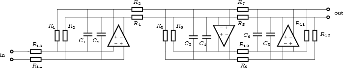
ci designThis will result in a file design.cir which is a SPICE netlist:
Circuit Description from FA
* Opamp Filter

.SUBCKT OPAMP 1 2 3 4
E1 3 0 1 2 1000
E2 0 4 1 2 1000
.ENDS OPAMP

* Integrator 1
C1 5 8 2.856667E-12
C2 6 7 2.856667E-12
X1 5 6 7 8 OPAMP
* Integrator 2
C3 9 12 2.856667E-12
C4 10 11 2.856667E-12
X2 9 10 11 12 OPAMP
* Integrator 3
C5 13 16 2.856667E-12
C6 14 15 2.856667E-12
X3 13 14 15 16 OPAMP

* Resistors
* From A
* A(0, 0)
R1 8 5 66530.9
R2 7 6 66530.9
* A(1, 0)
R3 8 9 41721.4
R4 7 10 41721.4
* A(1, 1)
R5 12 9 133062
R6 11 10 133062
* A(1, 2)
R7 15 9 47453.8
R8 16 10 47453.8
* A(2, 1)
R9 12 13 51264.9
R10 11 14 51264.9
* A(2, 2)
R11 16 13 133062
R12 15 14 133062

* From B
* B(0)
R13 5 1 66530.9
R14 6 2 66530.9

* From C
* Output nodes: 15 and 16

VIN 1 0 AC 1
EIN 2 0 1 0 -1


.END
Figure 17 shows a schematic diagram of this filter. To determine the minimum output-stage class-A bias currents of the opamps, add a statement
output: bias;to the FA input file. This results in
Maximal input signal level: 1
Minimum output bias currents:
Integrator 1:     7.79983e-05 A
Integrator 2:     6.73408e-05 A
Integrator 3:     6.61878e-05 A
Total bias current: 0.000211527 A.